400-888-2483
 我的账户
我的账户


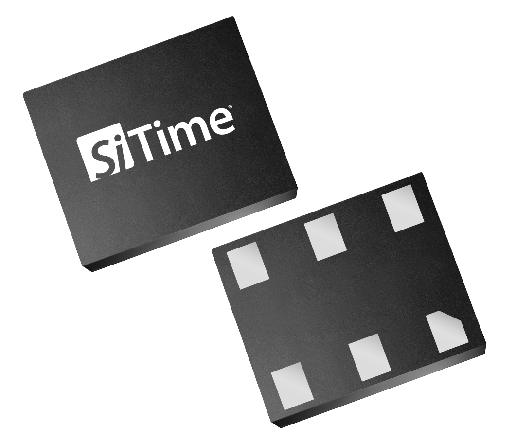
汽车级晶振
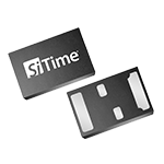
单端


差分
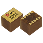
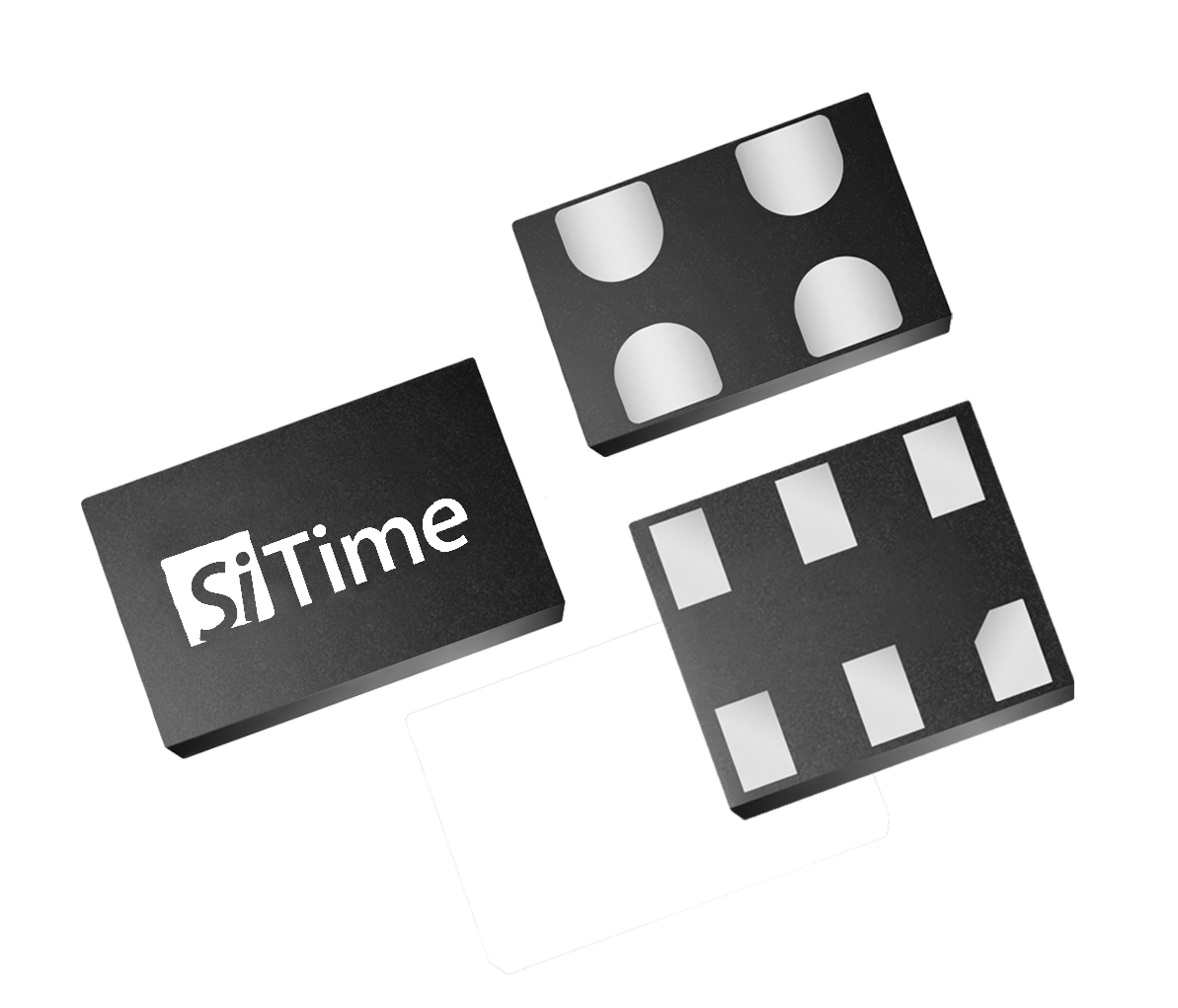
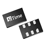
SiT9386
 1-220MHz任意频率,AEC-Q100,汽车级差分晶振LVPECL/LVDS/HCSL
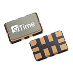
SiT9386
1-220MHz任意频率,AEC-Q100,汽车级差分晶振LVPECL/LVDS/HCSL
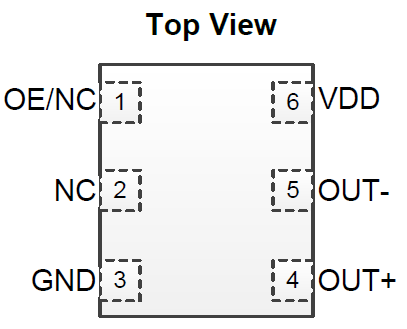
SiT9387
 -40~105℃,220-725MHz任意频率,LVDS/LVPECL/HCSL差分信号
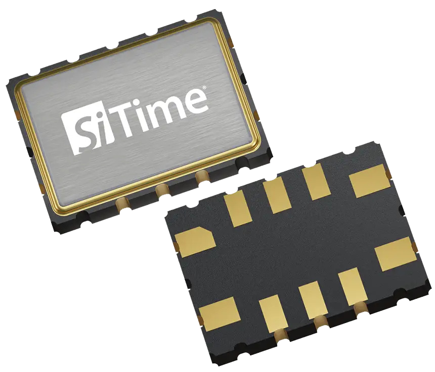
SiT9387
-40~105℃,220-725MHz任意频率,LVDS/LVPECL/HCSL差分信号
SiT9396
-40~125℃,1-220MHz任意频率,LVDS/LVPECL/HCSL差分信号
SiT9396
-40~125℃,1-220MHz任意频率,LVDS/LVPECL/HCSL差分信号
SiT9397
-40~125℃,220-920MHz任意频率,LVDS/LVPECL/HCSL差分信号
SiT9397
-40~125℃,220-920MHz任意频率,LVDS/LVPECL/HCSL差分信号


压控晶振VCXO
单端


0.23ps低抖动差分
SiT3372
 1-220MHz任意频率,HCSL/LVDS/LVPECL,最大±3200ppm牵引范围
SiT3372
1-220MHz任意频率,HCSL/LVDS/LVPECL,最大±3200ppm牵引范围
SiT3373
 220-725MHz任意频率,HCSL/LVDS/LVPECL,最大±3200ppm牵引范围
SiT3373
220-725MHz任意频率,HCSL/LVDS/LVPECL,最大±3200ppm牵引范围低成本差分

高精度温补晶振TCXO
±0.5ppm~2.5ppm


±0.1ppm~0.25ppm

SiT5501
 1-60MHz任意频率,±0.01ppm高精度,支持压控、数控、方波、削峰正弦波多种功能可选